
Inside TSMC’s 2026: Record Profits, A16 on Deck, and a Global Fab Buildout
TSMC’s record 2026: A16 angstrom node, global fab expansion in Arizona/Japan/Europe, and massive CapEx amid AI demand—what’s next for the chip titan.
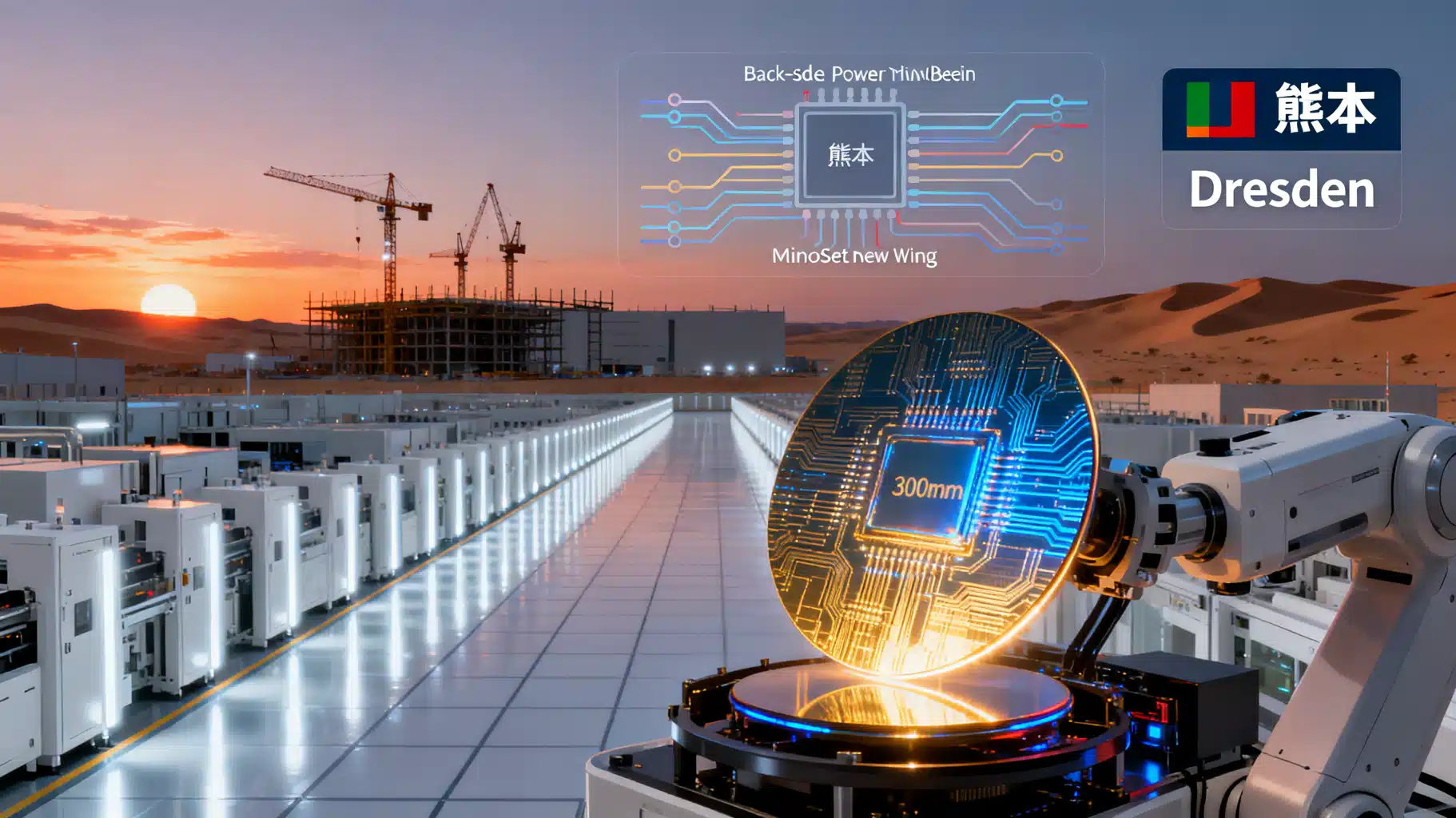
Image used for representation purposes only.
TSMC’s breakneck 2026: record profits, angstrom-class chips, and a global buildout
Taiwan Semiconductor Manufacturing Co. (TSMC) has entered late 2026 with record results, huge capital plans, and a rapid geographic expansion as AI demand continues to reshape the chip industry. On Oct 15, 2026, the company posted an all-time-high quarterly net income of NT$763.06 billion on revenue of NT$1,494.24 billion, and guided Q4 revenue to $52.3–$54.3 billion. Management kept 2026 capital expenditure at $60–$64 billion. (investor.tsmc.com )
The angstrom era arrives: N2 ramps, A16 targets 2H 2026
TSMC says its 2nm platform (N2) entered high-volume manufacturing in Q4 2025, with a fast ramp through 2026. The company’s next step is A16—an angstrom-class node that introduces a backside power delivery network branded Super Power Rail (SPR)—which TSMC has repeatedly targeted for volume production in the second half of 2026. (investor.tsmc.com )
TSMC’s 2026 technology symposium also highlighted N2U, a tuned variant that adds modest performance, power, and density gains over N2P via design-technology co-optimization. While TSMC’s official documents continue to place A16 in 2026, some industry analyses now expect A16’s broad availability to lean into 2027. (pr.tsmc.com )
At a high level, SPR moves power rails to the back side of the wafer, freeing the front-side metal for signal routing and reducing voltage droop—an approach expected to benefit large AI and HPC designs. TSMC’s public materials position A16 for these workloads. (cld.tsmc.com )
Arizona becomes central to leading‑edge capacity—and packaging
TSMC’s U.S. story accelerated in 2026. The company has pledged a further $100 billion to expand in Arizona, complementing earlier multi-fab plans around Phoenix, and has been evaluating additional U.S. sites, including Texas. TSMC also reiterated that 2026–2028 spending will be “significantly higher” than the past three years to support customers’ AI growth. (apnews.com )
On the technology side, TSMC plans to open an advanced packaging facility in Arizona by 2029, expanding U.S. capacity for AI-critical 2.5D/3D integration. This complements a long‑term partnership with Amkor to colocate advanced back-end services near TSMC’s front‑end fabs in Arizona—an arrangement intended to compress cycle times and localize end‑to‑end supply for U.S. customers. (investing.com )
TSMC’s own roadmap shows Arizona as part of its plan to build an independent GIGAFAB cluster in the U.S. At the same time, the company’s 2025 annual report confirms the first Arizona fab began 4nm volume production in late 2024, setting a baseline from which future 3nm and 2nm-class ramps can build. (investor.tsmc.com )
Japan’s 3nm pivot: Kumamoto Phase 2 wins approval
Japan moved from mature to cutting-edge logic in 2026. Tokyo formally approved a plan for TSMC’s Kumamoto Phase 2 to produce 3nm chips, with initial output of about 6,000 wafers per month and mass production targeted by 2028. This marks a major upgrade from the original 6–12nm plan and reflects Japan’s bid to anchor AI-era manufacturing onshore. (eetimes.itmedia.co.jp )
Phase 1 of JASM (TSMC’s Japan subsidiary) has been in mass production since late 2024 on 12/16nm and 22/28nm products for auto and industrial markets, but Phase 2’s N3 migration significantly raises the strategic stakes for Japan’s ecosystem. (taipeitimes.com )
Europe’s ESMC stays on schedule in Dresden
In Europe, construction of the European Semiconductor Manufacturing Company (ESMC)—a JV between TSMC, Bosch, Infineon, and NXP—in Dresden, Germany, remains on track. The project targets production by the end of 2027, focused on 28/22nm planar and 16/12nm FinFET capacity at roughly 40,000 wafers per month, strengthening regional supply resilience. (focustaiwan.tw )
Packaging is the new bottleneck—and battleground
The AI wave has shifted bottlenecks from front-end lithography to advanced packaging. Beyond the Arizona facility plans, TSMC continues scaling its CoWoS portfolio, including larger CoWoS‑L configurations. Company filings indicate 5.5‑reticle CoWoS‑L qualification completing in 2026 to meet rising compute-in-package performance targets. (investor.tsmc.com )
Policy friction: export controls and materials risk
Export-control turbulence remains a structural risk for TSMC and its customers. Over the last two years, TSMC has demonstrated strict compliance, including halting shipments to a client after parts were found in Huawei products, underscoring the complexity of indirect flows through third parties. (investing.com )
Meanwhile, Beijing’s restrictions on certain rare-earth materials have prompted TSMC to explore factory‑equipment alternatives (such as rare‑earth‑free motors) to reduce vulnerability in tool supply. The initiative, reported in October 2026, shows leading‑edge fabs hardening supply chains at the component level. (investing.com )
Demand picture: AI leads, N3 share climbs, and 2027 caution
TSMC’s 2026 outlook remains buoyed by AI infrastructure demand from U.S. hyperscalers and leading chip designers. Industry trackers expect N3 to surpass N5 as TSMC’s top revenue node in 2H 2026 as new smartphone and AI designs ramp, while the company itself forecasts full‑year 2026 sales growth above 40% in U.S. dollar terms. (trendforce.com )
Still, TSMC struck a prudent tone about 2027 macro uncertainty even as it logged a sixth straight record profit in Q3 2026. The firm kept 2026 CapEx at $60–$64 billion and reiterated that 2026–2028 investments will be “significantly higher” than in prior years to sustain technology leadership and meet customer roadmaps. (marketscreener.com )
What to watch next
- A16 production timing: Company materials continue to guide to 2H 2026; independent trackers suggest some slip into 2027. Either way, backside power’s rollout across AI/HPC designs is the architectural milestone to watch. (investor.tsmc.com )
- U.S. footprint: Concrete milestones on Arizona’s advanced nodes and the 2029 packaging plant, plus any movement on a potential Texas site. (investing.com )
- Japan’s N3 build: Ground progress, tool move‑in cadence, and supply-chain localization for Kumamoto Phase 2 ahead of the 2028 mass‑production target. (eetimes.itmedia.co.jp )
- Europe’s first TSMC fab: ESMC construction pace and partner ecosystem alignment into 2027. (focustaiwan.tw )
Bottom line: TSMC is converting the AI surge into record financials while racing to industrialize angstrom‑class logic, scale advanced packaging, and diversify manufacturing across the U.S., Japan, and Europe. The company’s execution on A16 and its overseas fabs will define the competitive landscape for the second half of this decade. (investor.tsmc.com )
Related Posts

Arm Stock Soars as Company Enters Silicon With First In‑House ‘AGI CPU’
Arm stock jumps after Arm unveils its first in‑house AGI CPU, entering silicon with Meta as lead partner and targeting agentic AI data centers.

AMD Stock after Meta’s 6GW AI Deal: Growth, Dilution, and the 2026 Playbook
AMD stock jumps as Meta inks a 6GW AI chip deal featuring performance-based warrants. Here’s what it means for growth, dilution, and 2026 execution.

Jensen Huang Under Fire: Nvidia Opens Probe Into Alleged Chinese Spy Targeting as Markets and Congress React
Nvidia CEO Jensen Huang admits affair as board probes reported Chinese spy plot. Congress seeks briefing Nov. 18 amid market, policy fallout.